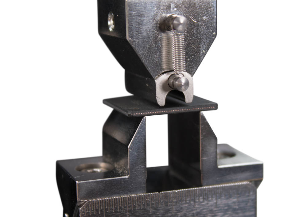
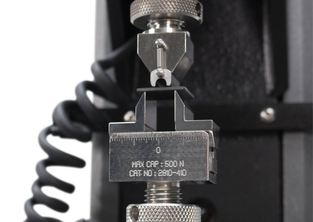
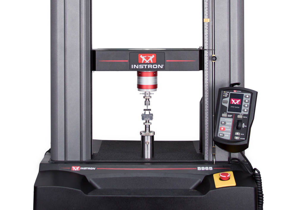
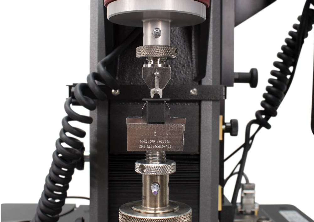
The Challenge
Understanding the mechanical reliability of microelectronic components and packages is a critical step towards design validation. With high density packaging, components are getting smaller and thinner so they can be used on the printed circuit boards (PCBs) of hand-held devices. Furthermore, new materials are being introduced, such as the addition of layers on electronic packages, which requires validation of the material’s strength. During new product development, OEMs are required to know the mechanical stress induced on various electronic packages, as they are subjected to warping from the assembly process of PCBs on the top and bottom of the substrate. New innovations in electronic packages, such as chip-on-film, stacked multi-layered packages, etc. require a thorough understanding of mechanical failure.